Surface plasmons are coherent and collective electron oscillations confined at the dielectric–metal interface. Benefitting from the inherent subwavelength nature of spatial profile, surface plasmons can greatly accumulate the optical field and energy on the nanoscale and dramatically enhance various light–matter interactions. The properties of surface plasmons are strongly related to materials and structures, so that metals, semiconductors and two-dimensional materials with various morphologies and structures can have alternating plasmonic wavelengths ranging from ultraviolet, visible, near infrared to far infrared. Because the electric field can be enhanced by orders of magnitude within plasmonic structures, various light–matter interaction processes including fluorescence, Raman scattering, heat generation, photoacoustic effects, photocatalysis, nonlinear optical conversion, and solar energy conversion, can be significantly enhanced and these have been confirmed by both theoretical, computational and experimental studies. In this review, we present a concise introduction and discussion of various plasmon-enhanced light–matter interaction processes. We discuss the physical and chemical principles, influencing factors, computational and theoretical methods, and practical applications of these plasmon-enhanced processes and phenomena, with a hope to deliver guidelines for constructing future high-performance plasmonic devices and technologies.


Over the past decades, surface plasmons (SPs) have attracted much attention due to its subwavelength spatial profile of modal field that can be harnessed to dramatically enhance light–matter interactions. 1,2,3,4,5,6,7,8,9 SPs are coherent and collective electron oscillations at the interface between two materials possessing positive and negative real part of dielectric functions respectively (e.g., metal–dielectric interface). SPs can be generally divided into two categories, i.e., localized and propagating SP polaritons (SPPs). Benefited from the greatly enhanced local electric field, SP can remarkably enhance the interaction strength between photons and materials, spurring the fast-growing developments of plasmon-enhanced fluorescence, Raman spectroscopy, heat generation, photoacoustics, photocatalysis, nonlinear optics, solar energy conversion, and so on.
In this paper, we briefly review recent progress on plasmon-enhanced light–matter interactions by design of plasmonic materials and structures. Firstly, we discuss SPs in metal, semiconductor, and 2D materials with various morphologies, structure regulations, and resonance wavelengths. Then we examine the principle of plasmon-enhanced light–matter interactions in the scope of hot spots and discuss in more details several relevant theoretical and computational methods that enable one to deeply understand these plasmon-enhanced phenomena and processes. Next, we introduce several representative applications of plasmonic materials, structures, and devices such as plasmon-enhanced fluorescence, Raman spectroscopy, heat generation, photo-acoustics, photocatalysis, nonlinear optics, and solar cells. Finally, we present summary and perspectives of plasmon-enhanced light–matter interaction.
SPs originate from coupling between photons and free electrons. Conventionally, SPs are investigated inside metals, such as noble metal gold and silver, with an abundant amount of free electrons and resonance wavelength located in the visible and near-infrared regions. Later on, heavily doped semiconductors and 2D materials are also demonstrated to exhibit abundant plasmonic responses. 10 Usually the plasmon frequency \(\omega _p\) is given by
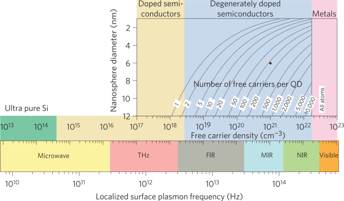
$$\omega _p = \left( <\frac<<4\pi Ne^2>>>> \right)^$$where N is the density of carriers (electrons or holes), m* is the effective mass of carriers. One can easily find that \(\omega _p\) is proportional to square root of N. Figure 1 shows the value of \(\omega _p\) for various materials and nanoparticle sizes. For noble metal nanoparticles, typical value of N is 10 22 –10 23 cm −3 and the plasmon resonance wavelength is in the NIR and visible region. For doped semiconductors, typical value of N is 10 16 –10 21 cm −3 and the plasmon wavelength is in the THz and NIR region. 11 As shown in Fig. 1, plasmon frequency can be tuned in a wide range by simply changing free carrier or doping density. Aside from the material properties, the plasmon resonance frequency and strength strongly depend on physical factors such as physical size, morphology, and geometrical arrangement. In the following text we will discuss SPs in different materials with various morphologies and structures.
Metals are popularly assumed to be excellent candidates for plasmonic applications. Among them Ag is the best material for plasmonics due to its lowest optical loss in the visible and NIR spectral ranges. However, Ag would oxidize quickly and suffers severe losses due to surface roughness. Au is another popular plasmonic material with excellent performance in the visible and NIR spectral ranges, and superior chemical stability under ambient conditions. As Ag and Au are very expensive, Cu and Al become alternative choices. However, Cu and Al both suffer from chemical instabilities under atmospheric conditions, restricting their further applications. Alkali metals are also ideal for plasmonic application, but they are so reactive to air and water that they must be stored in vacuum or inert gas. Therefore, Alkali metals are rarely used for plasmonics. Pd and Pt have attracted much attention owning to their applications in catalytic activities, although they are strongly absorptive in the visible wavelength and thus not good plasmonic materials. Besides pure metals, alloyed metals are broadly considered for plasmonic applications. The alloying of different noble metals can be used to tune the SP resonance (SPR) wavelength accordingly. For example, AuxAg(1−x) alloy nanoparticles display SPR over a broad range of the UV–vis spectra and SPR wavelength exhibits red shift while increasing particle size. The AuxAg(1−x) alloy nanoparticles with varying mole fractions show only one plasmon absorption and similar plasmonic strength as composite Gold and Silver. The plasmon band presents blue shift linearly with increasing mole fractions of silver. 12,13,14
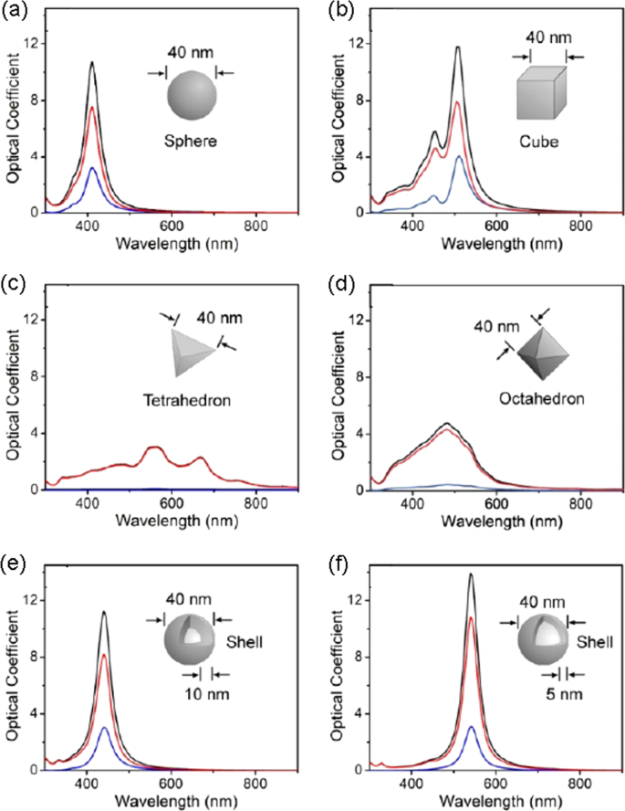
Another crucial aspect is to harness the geometric morphologies of metallic nanoparticles and nanostructures, which is popularly explored so as to shape and manipulate plasmonic properties. Figure 2 illustrates the calculation results of extinct, absorption, and scattering spectra for Ag nanoparticles with diversified geometric shapes (i.e., sphere, cube, tetrahedron, and octahedron) and topologies (i.e., solid, hollow, and core–shell). 15 This is an excellent example showing the strong relationship between plasmonic properties and morphologies of metallic nanoparticles.
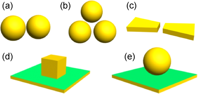
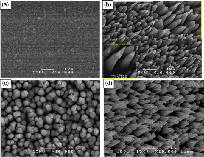
For practical applications such as fluorescence and Raman scattering, very large enhancement of local field intensity is highly desired to realize high-efficiency signal detection. Such local field enhancement can be readily found around sharp corners, edges and conical tips of metallic nanoparticles. In addition, appropriate structural arrangement of metallic nanoparticles can lead to larger enhancements. As shown in Fig. 3, plasmonic structures composed of multiple metallic structures, such as dimers and aggregates, have been designed and fabricated to promote plasmonic enhancements to a very high level. 9 Benefited from the huge enhanced field inside the nanometer gap, two groups reported single-molecule Raman signal detection in Ag nanoparticle aggregates in 1997, with an estimated Raman enhancement factor up to 10 14 –10 15 . 16,17 To relieve complex fabrication procedures, hybrid structures made from metallic nanoparticle placed on a metal substrate separated by a nanometer-thick dielectric thin film have been demonstrated to be efficient for plasmonic enhancements. An alternative structure for efficient Raman enhancement is shown in Fig. 4, which are Ag sharp nanoneedle arrays as fabricated by a simple Ar+-ion irradiation method and the Raman signal enhancement factor can reach ~10 10 . 18 Most recently, metallic nanoparticles hybridized with magnetic materials have been successfully developed, where the plasmonic response of metallic nanorod can be adjusted by simply changing the external magnetic field directions. 19
Heavily doped semiconductor materials exhibit metallic features and thus can be utilized for plasmonic applications. For heavily doped semiconductors (p- or n-type), the carrier density can be so high to exhibit metallic properties. For example, ReO3 type oxides, telluride or nitride materials have displayed extinct plasmonic properties in the visible and NIR region. Similarly, plasmonic features in semiconductor could be easily modulated by changing the shape, size, type, distribution of doped elements, and doping concentration of materials. 20 Considering distinct material properties of semiconductors from metals, SPs in semiconductors behave quite differently from SPs in metals. One promising feature of SPs in heavily doped semiconductors is relatively low loss compared with metals. For example, zinc oxide and indium oxide can be readily doped as high as 10 21 cm −3 , yet the loss is at least four times smaller than Ag in the NIR range. By increasing the doping concentration of semiconductor, the frequency of SP will shift towards higher energy. 21 Moreover, many semiconductors have unique anisotropic crystalline and thus optical feature, and would generate distinct plasmonic response along different crystal axes.
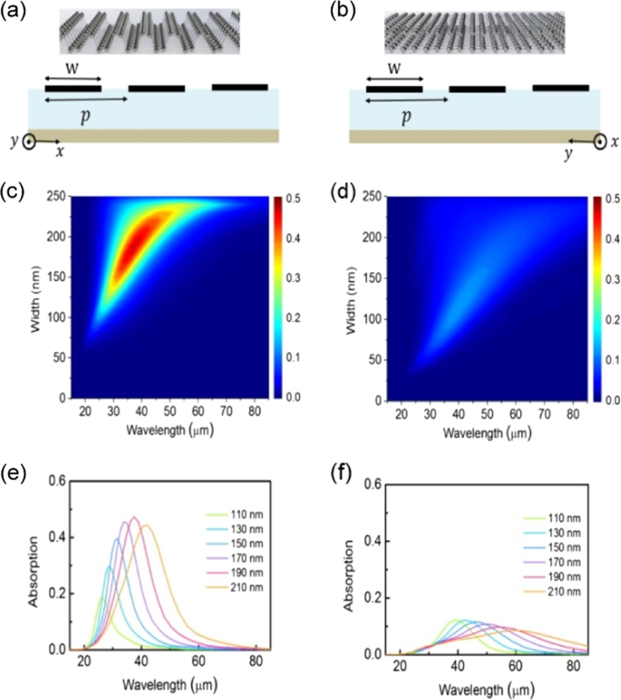
2D materials have recently become a hot and popular candidate class of plasmonic materials. For example, graphene, with ultrahigh carrier mobility, could have electrically tunable plasmonic feature in the mid-infrared and terahertz regions. 22 Compared with other bulk materials, SPs in 2D materials are highly confined spatially and the corresponding dispersion relationship is far away from the light line (such as Dirac plasmons in graphene 23 ). Therefore, the wavelengths of polaritons in 2D materials are highly squeezed, such as wavelengths of plasmon polaritons in grapheme nanoribbon arrays 24 and phonon polaritons in BN nanoribbon arrays 25 are squeezed by a factor over 100. Broadband all-angle negative refraction of highly squeezed hyperbolic polariton in an infrared regime were realized. 26,27 Due to the high-effective refractive index of highly squeezed polaritons, the superlight inverse Doppler effect can occur with a relatively small value of v (the condition of superlight inverse Doppler effect: \(v = \frac>\) ). 28 In addition, benefited from the multimode resonance of phonon polaritons at multiple frequencies in naturally anisotropic 2D materials (such as hexagonal BN), multifrequency super-scattering was found in this subwavelength hyperbolic structure. 29 Taking the advantage of flexibility in tuning the chemical potential in 2D materials, it is also possible to realize tunable directional excitation of highly squeezed polaritons, and complete active control of the near-field directionality of plasmons. 30 In order to keep the degree of confinement and avoid plasmonic scattering at edges, 2D materials could be rolled into a cylinder so as to produce low-loss plasmons with higher field confinement, such as carbon nanotubes. 31 Moreover, the plasmon dispersions of p- and n-doped 2D materials behave very differently, owning to the asymmetry in the electron–hole carrier concentrations. The overall plasmonic response of 2D materials is weaker than metals due to the atomic thin dimension. However, the plasmonic effect of 2D materials can be effectively enhanced through electrostatic or chemical doping techniques. By changing the carrier concentration with external electric gates, the dispersion and lifetime of SPs in 2D materials can be readily tuned. Besides, chemical doping in 2D material would also influence plasmonic features. For example, the inherent plasmon resonance of 2D MoS2 lies in the far-infrared and terahertz range. Through Li + ion doping, 2D MoS2 can become a semimetallic state and the plasmon frequency would shift to the visible and ultraviolet range. 32 The multiplied photocurrent response is obtained by coupling few-layer MoS2 with Au plasmonic nanostructure arrays owning to the localized SP resonance. 33 In addition to doping, morphology of 2D materials will also influence the plasmonic effect. For monolayer black phosphorus nanoribbons arrays along the armchair and zigzag directions, it was found that they displayed polarization-dependent anisotropic plasmonic response at mid-infrared and far-infrared wavelength regime (as shown in Fig. 5). 34
SP allows for efficient transport and localization of optical energy at nanoscale, and these nanoscale regions are popularly called as hot spots. As discussed previously, the electric field can be readily enhanced by orders of magnitude upon the incident light by carefully designing plasmonic structures. Therefore, significant enhancement of light–matter interaction can be readily expected at these hot spots. For instance, an enhancement of light intensity by 10 5 could give rise to a Raman enhancement factor by 10 10 . Besides, both mesoscopic and microscopic strategies should be carefully considered and manipulated in order to maximize the enhancement of light–matter interactions. On the mesoscopic level, one should engineer and thus optimize the morphological and structural configuration of plasmonic platforms so as to maximize the electric field enhancement. Usually metallic nanostructures with sharp corners and edges are preferred to have strongly localized electric fields. Meanwhile, metallic nanostructures with high density of hot spots, e.g., sea urchin-like particle, 35,36 have been fabricated in order to have as many hot spots as possible. On the microscopic level, one should build clear picture and obtain deep understanding of key microscopic factors regarding the light–matter interaction strength, either from classical or quantum aspect. What is more, in some cases one should consider these two scopes simultaneously. A typical example is in a plasmonic nanogap one must consider the critical role of molecule Rayleigh scattering in contributing to Raman scattering, which are two basic microscopic light-molecule interaction processes, due to the multiple mesoscopic scattering of light with the plasmonic nanogap. In many situations other factors such as quantum plasmonics correction should also be carefully taken into considerations. 9 Usually the electromagnetic enhancement factors are obtained while neglecting the quantum plasmonics effect. However, this is not valid. The reason is that the surface layers of metallic structures generally behave in a much weaker plasmon resonance compared with the inner bulky metallic material, thus practical electromagnetic enhancement factors at these hot spots are much less than the value estimated by means of pure classical electrodynamics.
To fully and deeply understand all important properties of SP in various materials and structures, including transport dispersion and modal profile, field localization, and enhancement, and their classical and quantum interactions with various macroscopic, mesoscopic, and microscopic objects, it is pivotal to employ theoretical and computational methods and tools to construct basic and detailed pictures of these subjects, meanwhile closely cooperating with experimental and technical researches. These methods can be categorized into two major disciplines. The first is based on classical physics, which uses classical optics, electromagnetism, and electrodynamics to calculate the basic properties of SP. The second is based on quantum physics, which includes (1) using condensed matter physics to calculate the accurate plasmonic response of metal materials and structures and account for the so-called quantum plasmonic correction effects; 9 (2) using quantum mechanics to account for the optical interaction of SP with molecules, quantum dots, excitons, etc.; (3) using quantum chemistry to account for surface electron excitation, transport, transfer, and their influence to the optical properties (fluorescence, Raman, etc.) of molecules. In this regard, light–matter interaction in plasmonic materials and structures is a multiple-disciplinary area of very rich basic physics and chemistry, and collective and cooperative efforts from diversified community must be made to advance this research area.
The excitation and transport of SP in metal nanoparticles and nanostructures can be well understood from Maxwell’s equations, which can be accurately calculated and simulated by using several rigorous numerical approaches and computational software packages such as discrete-dipole approach (DDA), finite-difference time-domain method (FDTD, e.g., software package FDTD solution), and finite-element method (FEM, e.g., software package COMSOL). The plasmonic response of a metal nanoparticle is well characterized by the extinction, scattering, and absorption cross-section ( \(C_,C_,C_\) ) and normalized coefficient ( \(Q_,Q_,Q_\) ) with respect to the apparent effective area ( \(S_\) ). For a tiny particle with size (radius r) far smaller than the incident light wavelength, the plasmonic response can be modeled by an electric dipole moment as \(<\mathop<<\mathbf
>>\nolimits> = \alpha <\mathbf
$$\alpha = r^3[(\varepsilon _m(\omega ) - \varepsilon _d)/(\varepsilon _m(\omega ) + 2\varepsilon _d)]<,>$$
is the particle polarizability, with \(\varepsilon _m(\omega )\) and \(\varepsilon _d\) being the dielectric constant of metal and background medium. Let \(k = 2\pi n_0/\lambda\) ( \(n_0\) being the refractive index) be the wave vector of light in the background medium, one can find
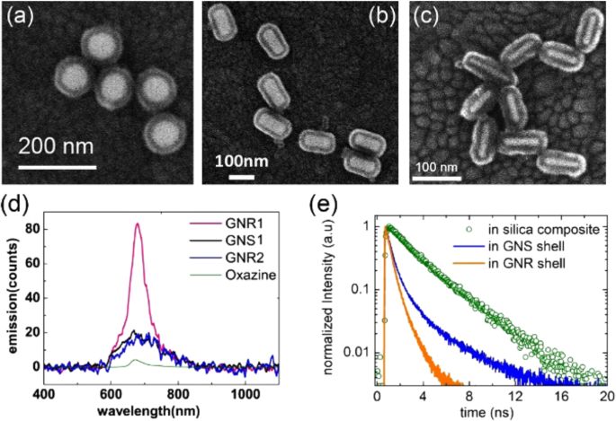
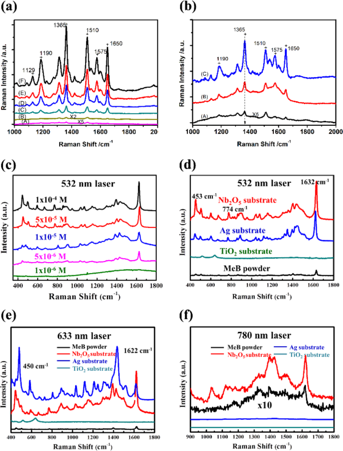
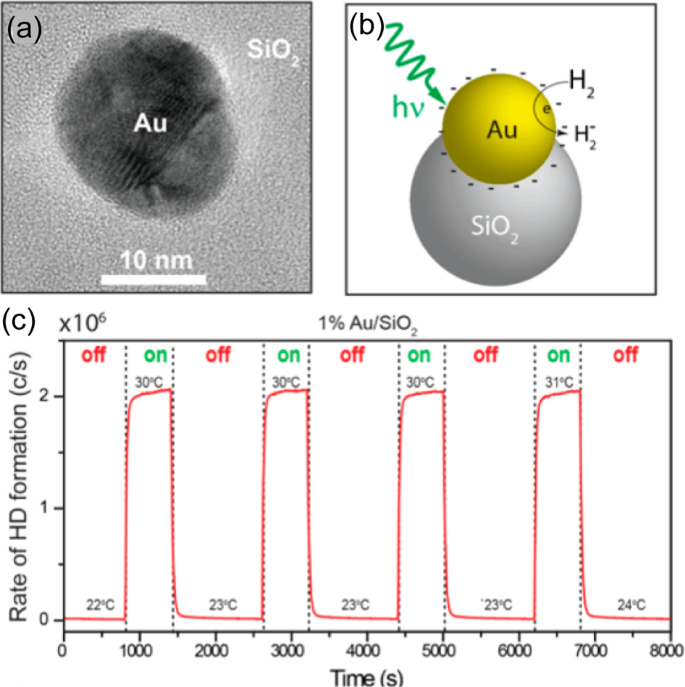
$$C_It is easy to find that when \(\varepsilon _m(\omega ) + 2\varepsilon _d \to 0\) (more precisely \(<\mathrm >>\nolimits> _i(i = 1. N)\) located at position \(<\mathop<<\mathbf >>\nolimits> _j = \alpha _j<\mathop<<\mathbf The extinction, scattering, and absorption spectrum can exhibit one or more SPR peaks, and their physical origin (dipole or quadrupole modes, polarized charge distribution, and accumulation profile, local field distribution and enhancement profile) can be well analyzed by DDA, FDTD, FEM, and other numerical tools. The crucial quantities to describe SPP propagating at a metal–dielectric interface are dispersion \(k_ = F(\omega )\) , modal profile \(<\mathop<<\mathbf From these formula, SPP in various plasmonic materials and structures can be estimated and compared. It can be found that in the visible and near-infrared wavelength regimes, for most metals, even noble metals as Au and Ag, the decay length \(\delta _\) of SPP is on the order from several tens micrometers to several micrometers, indicating the vast difficulty to construct a large-scale integrated optical devices and circuits in the platform of plasmonic materials. It can also be found that for 2D materials such as graphene, the field localization length is on the order of 10 nm, 2–3 orders of magnitude smaller than the SPP wavelength 7–8 μm, indicating an extremely tight confinement of field at the surface of 2D materials. The excitation of localized SPP in metal nanoparticles and propagating SPP in metal thin film surface brings an excellent opportunity to squeeze electromagnetic energy from the incident light into the deep subwavelength space of SPP mode. This means greatly increased optical energy density and thus enhanced light–matter interaction in this nanoscale SPP modal space. Basically, this is simply the physical origin of engineering SPP dispersion and modal field to enhance various light–matter interaction. According to Eqs. (2)–(4), the condition to excite SPR and SPP and the degree of field localization and enhancement sensitively depend on the dielectric constant \(\varepsilon _m(\omega )\) of metal particles and structures in addition to their geometric shapes. In some special geometries, e.g., plasmonic nanogap in metal particle dimers and TERS, this \(\varepsilon _m(\omega )\) sensitivity is further enhanced for orders of magnitude. In these situations, quantum plasmonics effect play an important role, where electrons in top atomic layers of metal will have much weaker plasmonic response compared with in bulk, leading to much weaker local field enhancement factor at the surface of metal. 9 Therefore, it is critical to determine accurately the material dielectric response \(\varepsilon _m(\omega )\) in order to correctly evaluate plasmonic response of these vicinity atom/electron layers of metal. This requests very careful, deliberate and smart modeling and simulation of surface atom configuration, electron energy diagram and density distribution, and their optical response in terms of \(\varepsilon _m(\omega )\) , which obviously needs to learn experiences and expertize from condensed matter and materials physics. For instance, the first-principles calculation method based on density functional theory can be adopted to calculate the dielectric function spectra and optical absorption spectra of materials by CASTEP program package. The accurate knowledge of plasmonic response, local field distribution, and enhancement will set a solid basis to further study various plasmon-enhanced light–matter interaction processes and problems, such as molecule fluorescence, Raman scattering, plasmon-exciton strong coupling, hot-electron assisted optoelectronics, and photocatalysis. These processes involve fruitful physics and chemistry. To get a correct and accurate picture of plasmon-enhanced light–matter interactions, one inevitably need experiences and expertize from atomic, molecular and optical physics, semiconductor physics, optoelectronics, molecular chemistry, and surface chemistry. Moreover, take a single problem as example, molecular Raman scattering involves a series of physical and chemical processes that might either be basically separate and independent or be strongly coupled and intertwined with each other, making the accurate theoretical understanding even more difficult and challenging. As such, advancement of plasmon-enhanced light–matter interaction at nanoscale or single-molecular scale urgently calls for more efficient theoretical and numerical concepts, methodologies, and tools. Plasmon-enhanced fluorescence has extensively been experimentally investigated, and has become one of the most important surface-enhanced spectroscopy techniques. 37 Fluorescence from a fluorophore can be generally characterized in terms of quantum yield and lifetime. Either excitation or emission of light emitter can be enhanced by plasmon resonance. To reach maximum excitation-emission efficiency, many experiments have been dedicated to manipulate the SP frequency between peak excitation wavelength and peak emission wavelength of fluorophore. 38,39 For plasmon resonance close to the peak of excitation wavelength, excitation light can be well confined and highest excitation efficiency can be expected. While for plasmon resonance close to the peak of emission wavelength, highest emission efficiency can be expected once the distance between fluorophore and plasmonic structure is optimized. Generally, the peak of excitation wavelength differs from the peak of emission wavelength, thus one has to make compromise between the optimum excitation efficiency and optimum emission efficiency. By taking advantage of double plasmon wavelengths (i.e., longitudinal and transverse plasmonic modes) inside an Au nanorod structure, it is therefore possible to have maximum enhancement of excitation and emitting efficiency. 40 As shown in Fig. 6, one specific kind of Au nanorods, whose transverse and longitudinal plasmon wavelengths are matching with the excitation wavelength and emission band of Oxazine-725, exhibit the most favorable performance in both intensity and lifetime of fluorescence. Besides, the combination of SPs and state-of-the-art fabrication techniques can fundamentally change and improve the ability of fluorescence technology. 41 Raman scattering is one type of well-known nonlinear light–matter interaction processes, where photons couple with intermolecule vibrational and rotational motions. 42,43 Therefore, Raman spectroscopy provides versatile tools for investigating molecular vibrations and works as fingerprint for precise chemical analyses and molecular identifications. However, Raman scattering cross-section is extremely small compared with fluorescence process, which is usually 15 orders of magnitude smaller. To promote Raman spectroscopy and make it practically applicable, it is highly desirable to develop enhanced Raman spectroscopy with ultrahigh sensitivity even down to single-molecule level, which is quite appealing for both fundamental research and industry applications. SP is ideal for enhancing Raman scattering processes. As shown previously, the energy of light can be strongly localized at the hot spots on the surface of metallic nanostructures, so that the light-molecule Raman interaction strength is remarkably enhanced. Specifically, plasmon-enhanced Raman scattering are intensively studied in two categories, surface-enhanced Raman scattering (SERS) and tip-enhanced Raman scattering (TERS). 44,45,46,47,48,49,50,51,52,53,54 As a result of huge enhancements contributed by SP resonance, the detection level of Raman scattering could be promising to reach the single-molecule level. Below we will discuss several strategies to promote the plasmonic enhancement of Raman scattering. Theoretically, we could obtain total enhanced Raman scattering intensity as follows: 9 where \(A\) represents Raman signal collection efficiency of optical systems, \(G(<<\mathbf Specifically, we could optimize the morphology of plasmonic nanostructures to enhance Raman scattering. Generally, the Raman enhancement factors by gold nanoparticles are only at the level of 10 6 , which is far below the level needed for achieving single-molecule Raman detection. As shown previously, plasmonic nanoparticles with sharp corners or tips are favored to give rise hot spots with more significantly enhanced field. 55,56,57,58,59,60,61,62,63,64,65 Nanoparticle with cubic, rectangular, and conical morphologies have been synthesized for further boosting Raman enhancements. Especially for the conical tip geometry, such as the sea urchin particles and nanoneedles (as shown in Fig. 7a, b), giant Raman enhancements as strong as 10 10 could be reached. 36,66 Furthermore, metallic nanogap geometry (such as metallic nanoparticles dimers and aggregates) have been proposed for enhancing Raman scattering process, since mutual plasmonic coupling between adjacent plasmonic nanoparticles could provide electric field enhancement significantly. It is remarkable that by using this giant Raman enhancement mechanism in 1997 two groups reported successful detection of single-molecule by Raman spectroscopy in silver nanoparticle aggregates. 16,17 Aside from the optimization of morphology, introducing gain materials into plasmonic nanostructures could be another channel for enhancing Raman signals. 67,68 By incorporating gain medium into gold nanorods, Raman enhancement factor as large as 10 16 could be reached at hot spots. 68 Moreover, doped semiconductors also provide exceptional route for plasmon-enhanced Raman spectroscopy. As shown in Fig. 7c, Raman spectra of MeB molecules with concentrations in the range of 1 × 10 −4 to 1 × 10 −6 M has been successfully detected on Nb2O5 substrates. Benefited from plasmonic enhancements, the detection limitation can be as small as 10 −6 M upon the irradiation of 532 nm laser. The irradiation laser also has an important effect on the intensity and position of vibrational bands. Via changing the excitation laser, many bands for solid MeB do not appear in the spectra. Especially, for 780 nm irradiation laser, only two bands located at 1614 and 1394 cm −1 can be recognized. Therefore, the Nb2O5 semiconductor substrate could effectively attenuate the fluorescence effects and enormously enhance the Raman signals of MeB molecules. It is worthwhile to note here that the classical theory of Raman scattering could not provide convincing explanations regarding the single-molecule Raman scattering observations 16,17 or the TERS experiment of subnanometer chemical mapping of a single-molecule inner structure. 69 Unlike the theoretical model that uses a 1-nm spot size of light for activating Raman signals, 69,70 it is found that the microscopic Raman mechanism is strongly related to the Rayleigh scattering. 71,72,73 It has been proposed that multiple Rayleigh scattering between the Raman molecule and metallic nanostructures will notably modify the localized electromagnetic background and this modification would inversely alter the local field around the molecule significantly, so that Raman activation and radiation processes would be dramatically enhanced simultaneously. In subsequent theoretical studies, it is shown that the localized multiple Rayleigh scattering effect could reduce the size of hot spot down to 1.3 nm, thereafter making it possible to identify the adjacent atoms in 1 nm separation by Raman mapping. Further theoretical studies demonstrated that Raman enhancement could reach 10 14 –10 15 by introducing the mechanism of Rayleigh scattering in SERS involving plasmonic dimers and aggregates, which implies that Raman spectroscopy could readily identify single-molecule by using these SERS substrates. As is known, hot electrons can be efficiently excited due to plasmon-enhanced photon absorption. Heat is thus significantly generated as a result of electron–phonon interactions, leading to a promising new arena of thermo-plasmonics. 74,75,76 Various metallic nanostructures have been carefully designed to control local or global temperature remotely with the use of light illuminations. To act as ideal sources of heat, SP has enabled various potential applications, such as photothermal melting of nanomaterials 77,78,79,80,81,82,83 nanofluidics, 84,85 photoacoustic, 86,87,88 and photothermal imaging, 89,90,91 cancer therapy, 91,92,93,94,95,96,97,98 drug delivery, 99,100 nanotherapeutics, 101 and steam generating. 102 Photothermal effects are strongly related to photon absorption and electric field confinements, so it is desirable to carefully optimize the morphology of plasmonic nanostructures. 103 It has been found that one has to keep the associated electric fields inside the metal as much as possible. This point is readily understandable, since heat can only be generated as electrons interact with phonons inside metal materials. As a result, nanogap enhanced light field concentration, where the electric field is mostly located outside the metal, and does not help in increasing photothermal efficiency. Furthermore, Baffou et al. 103 found that small, flat, elongated, or shaped metal particles appeared to be better candidate for microscopic heat sources. When metallic nanoparticles are under light illuminations, local heat will be generated and the temperature of surrounding environment will subsequently rise. The temperature increase would be accompanied by slight change of refractive index in a quite small volume. Subsequently, a photothermal microscopy technique was proposed and successfully realized the imaging of metal particles with nanometer size accuracy. 89 The strongly localized changes of refractive index around the metal nanoparticles are recognized as the nanolens effect, 104 which can be effectively distinguished by phase differential measurements with enhanced sensitivity. 105 The employment of metallic nanoparticles for microscopic imaging has several advantages over conventional fluorescent markers, including free of fluorescence bleaching, blinking and saturation. People have already succeeded in protein tracking in vivo by taking the advantage of fluorescence bleaching absence. 106 Another promising application of thermo-plasmonics is for cancer therapy. Plasmonic particles, such as gold nanoparticles functionalized with small antibodies for specifying targeted cancer cells, entered live body and preferred to accumulate at cancer beds. 107 Upon excitation of near-infrared laser, normal tissue turned to be transparent while excitation laser was strongly absorbed by the specifically designed plasmonic nanoparticles and converted into heat efficiently. As long as the localized photothermal heating was strong enough, it would induce cellular hyperthermia and cause associated cell death and tumor remission. For example, gold nanocages (~45 nm in edge length) were successfully fabricated with strong absorption in the near-infrared region. 95 The absorption cross-section of such nanocages was numerically determined as large as 3.48 × 10 −14 m 2 , making gold nanocages perfect candidate for efficient conversion of NIR illumination into heat. Upon pulsed laser illuminations, biological materials would absorb the laser light energy, which will be converted to heat via nonradiative channels such as vibrational relaxations. Unlike heat induced refractive index change as discussed previously, generated heat will also lead to pressure buildup inside the media and yield generation of ultrasound waves. Then the outgoing acoustic waves can be collected by a conventional ultrasound transducer and transferred to electrical signals for reconstructing photoacoustic tomography or microscopy images. 88 As the excitation laser is only dedicated for heat generation rather than imaging, such induced acoustic waves would reach deep biological tissues (benefitting from its less scattered behavior) and provide in-depth and high contrast information. Specifically, the degree of contrast strongly depends on the conversion efficiency of photon-to-acoustic interaction processes. Apparently, it is crucial to have as large absorption cross-section as possible for enhancing the photoacoustic processes. Metallic nanoparticles appear to be ideal for photoacoustic imaging with enhanced performance, owning to their unique plasmonic features, as it can act as an efficient nanoscale heat source. Furthermore, metallic nanoparticles are biocompatible and easily functionalized by biomarkers with molecular specificity. 108 The first application of metallic nanoparticles (i.e., 40-nm spherical gold nanoparticles) for enhanced photoacoustic imaging was demonstrated in vitro experiment in 2004 109 and later in vivo. 110 Currently, metallic nanoparticles, such as gold nanocages, nanorods, and nanoshells, have all been successfully applied for enhanced photoacoustic imaging. 76 As a good example, gold nanocages have been investigated as one potential contrast agent for photoacoustic imaging in vivo. 110 Compared with gold nanoshells, gold nanocages show the advantage of larger absorption cross-sections that is very suitable for photoacoustic imaging. Moreover, the surfaces of nanocages are easier to bioconjugated with poly-(ethylene glycol) (MW = 5000), which could suppress immunogenic reactions and keep them long circulating in vivo. In the in vivo experiments, gold nanocages were injected into the rat circulatory system (three successive administrations, each dose of ~0.8 × 10 9 nanocages/body weight). With an 804-nm laser illuminations, photoacoustic imaging was performed immediately after each injection and continued for over five hours. Compared with reference results taken before the injection, one can easily conclude that the optical contrast was significantly improved, as shown in Fig. 8. By integrating signals obtained in the photoacoustic images and normalized to the reference results, up to 81% enhancement was found after two hours of third injection. Theoretical investigation demonstrated that gold nanocages had greater absorption cross-sections compared with gold nanoshells, which would favor for enhancing photoacoustic imaging. To further increase the contrast, gold nanorods with silica-coated shell have been successfully fabricated, aiming to manipulating the interfacial thermal resistance with surrounding environments. 111 With the silica coating, gold nanorods can act as photoacoustic nanoamplifiers, which significantly enhanced the efficiency of photon-to-acoustic conversion and gave rise to higher contrast photoacoustic signals. For early cancer detections and cancer cellular dynamics investigations, microscopic imaging of single cancer cells is highly desirable. However, this requires extremely high sensitivity and resolution of photoacoustic imaging. Furthermore, specially functionalized gold nanoparticles have been developed in order to realize microscopic imaging of single cancer cells. 112 It is well-known that chemical reactions are influenced by many factors, including pH, pressure and temperature. Therefore, SP appears naturally to act as efficient photocatalyst of chemical reactions at nanoscale, such as water splitting, 113,114,115 CO2 reduction, 116 and water purification. 117 Upon light illuminations, hot carriers (i.e., hot electrons or holes) would be generated firstly, then excite electronic or vibrational states of nearby or adsorbed molecules before hot electrons interacts with phonons (i.e., heat generation), and this will significantly accelerate the chemical reactions rate. 75 One typical example is dissociation of H2 on gold nanoparticle surfaces at room temperature, which is driven by hot electrons generated. 118,119 Gold colloidal nanoparticles (with diameters around 137 nm) were prepared and placed on SiO2 substrate, while reactant D2 gas was used to monitor H2 dissociations (H2(g) + D2(g) → 2HD(g)). A supercontinuum laser source was used to excite local plasmon resonance of gold nanoparticles. As mixed gas was flowing into the chamber, excited plasmon of gold nanoparticles generated hot electrons and transferred to H2, which populated the antibonding orbits of H2 and boosted the dissociation rates. The rate of HD formation was simultaneously recorded with laser turn on and off consecutively (as shown in Fig. 9). It clear shows that HD formation rate was significantly increased by 150 times with the pump laser on. 119 After changing the substrate from TiO2 to SiO2 and Al2O3, it was confirmed that H2 dissociation took place on the surface of gold nanoparticles rather than on the nanoparticle/substrate interface. 119 Thermal effect is another factor that significantly influences photocatalysis. It is well-known that temperature increase usually accelerates chemical reaction rate according to empirical Arrhenius law. In the previous section, we have shown that plasmon can be regarded as one kind heat source with localized space and controllable temporal behavior. Therefore, plasmon induced thermal effect could be expected to efficiently assist chemical reactions locally. For example, rhodium (Rh) nanoparticles have already been regarded as effective thermal catalyst due to plasmon induced heat generation. 120,121,122 However, in order to understand the microscopic mechanism of plasmon-induced photocatalysis, CO2 methanation reaction was carefully designed to distinguish contributions from thermal (including photothermal heating or thermal gradients) and nonthermal (including hot-carrier driven reactions, photo modification of the catalyst, or enhanced near-field effects) origins. 123 Experimental results revealed that both thermal and nonthermal mechanisms matter for significant photocatalysis effects. 123 Furthermore, an ultrafast surface-enhanced Raman thermometry technique was applied so as to understand the dynamics of photocatalysis on the ultrafast time scale. 124 Surprisingly, it was concluded that plasmonic photocatalysis was not primarily due to the thermal contribution, since ultrafast measurements revealed that energy quickly dissipated from the adsorbates into the surroundings in an ultrafast manner (less than 5 ps). 124 It is believed that better understanding of the underlying mechanism will be crucial for future designing highly efficient plasmonic enhanced photocatalysis techniques. Nonlinear optical effects are crucial for the rapid developments of modern optics. Generally, optical nonlinearity is an intrinsic weak effects, but can be significant as long as interacting electromagnetic field is fairly strong, due to the fact that nonlinear optical effects should depend superlinearly on the electromagnetic fields. 42,43 In various plasmonic structures, electromagnetic fields are highly localized thus could greatly enhance nonlinear optical conversions, giving rise to a new research field, namely nonlinear plasmonics. 125,126 Nonlinear optical processes, such as SERS, second harmonic generation (SHG), third harmonic generation, and multiphoton photoemission, have been demonstrated with enhanced performance in plasmonic structures. To be noted here, one important nonlinear optical effect, i.e., SERS, has been discussed thoroughly in the previous sections, thus will not be included in the following discussions. As is known, nonlinear optical effects are closely related to material symmetry. While third-order nonlinearity exists in all materials, second-order nonlinearity is only available in noncentrosymmetric materials. According to theory, localized electric fields mostly lie in the vicinity of metallic surface because of the plasmonic skin depth effect, thus the surface layer of metal and surrounding environment (such as adsorbed molecules) become crucial for plasmon-enhanced nonlinearities. As prominent plasmonic metals (such as gold, silver and aluminum) are all centrosymmetric with a face-centered cubic unit cell, they only enable bulk third-order nonlinearity in most situations. 126 However, SHG signals were readily observed and measured from these metallic structures in the early days of nonlinear optics history, as a result of broken symmetry at the metal surface. 127,128 This surprising discovery has led to the developments of metallic surface-enhanced SHG later on. It was further confirmed that rough metallic surface structures could lead to stronger localized electric fields, and larger enhancement of nonlinear optical effects could be observed. 129,130,131 Both the surface and bulk contribution to SHG from metallic surfaces were carefully identified and investigated. 125,132 Moreover, nonlinear interactions of SPs were also studied. 133,134 This plasmon-enhanced SHG was readily generalized to sum frequency generation, particular surface vibrational spectroscopy, in order to study information of adsorbed molecules on metal surfaces. 135,136 For example, with the help of surface vibrational spectroscopy and plasmonic resonance at electrochemical interfaces, in situ and real-time vibrational spectra were measured, revealing the electrochemical reaction process of how the surface was oxidized and reduced every cyclic voltammetry cycle. 137 Nonlinear optical effects in metamaterials or metasurfaces have attracted intensive interest recently. 138,139,140,141,142,143,144 The periodic metallic arrays, treated as artificial meta-atoms, have been demonstrated in various applications, including frequency selectivity, wavefront shaping, polarization control (including optical chirality), nonlinear geometric Berry phase, terahertz nonlinear optics and quantum information processing. 143,144 These exciting findings all lead to light–matter manipulation in more compact and effective manners. Aside from the above discussions, SPs could be highly sensitive to the dielectric properties of metals and surroundings. Therefore, it can bring opportunities for plasmonic sensors and ultrafast switching. 140,145 Finally, we focus on plasmon enhancement of photovoltaic efficiency. To satisfy increasing demand of energy, solar cells provide clean conversion from solar energy to electric energy without any negative impact (such as carbon costs) on the environment. 146 Therefore, it is desirable to develop high-efficiency photovoltaic techniques. By incorporating plasmonic metals into solar cells, one may expect overall performance improvements, such as increasing of light harvesting efficiency, tunablility of absorption spectra, and increasing of charge carrier separation efficiency. 147,148,149,150,151 The mechanism behind the plasmon-enhanced photovoltaic efficiency can be understood as follows. Firstly, hot carriers will be generated upon light illumination from the plasmonic structures. In a quite short time (~fs), generated hot carrier (e.g., electron) will transfer to surroundings (e.g., semiconductor), resulting in the spatial separation of charge and lowering the rate of electron–hole recombination rate. Secondly, as light is harvested by the metallic structures, electric field will be strongly localized on the surface of metal, consequently enhancing the photon absorption cross-sections significantly. Through combination of metallic structures with different morphologies or materials, the absorption cross-sections could be enlarged over broader spectra. 152,153 Thirdly, multiple scattering effects due to metallic structures will increase the optical paths of incident photons while going through the photovoltaic devices. And this will surely increase the absorption efficiency and improve the photovoltaic conversion performance. By carefully optimizing morphologies, concentrations, and geometric position inside devices of metallic structures, high-performance solar cells can be readily obtained with cooperation of plasmon and the rise of new organic compounds, such as perovskites. In summary, we have briefly while systematically reviewed the recent progress of plasmon-enhanced light–matter interaction by means of designing optimum plasmonic materials and structures. SPs in metal, semiconductor and 2D materials with various morphologies and structures, are discussed, with plasmonic wavelengths ranging from ultraviolet, visible, NIR to far infrared. We then discuss the principle of plasmon-enhanced light–matter interactions and the role of plasmonic hot spots. Representative applications of SPs, including plasmon-enhanced fluorescence, Raman spectroscopy, heat generation, photoacoustic, photocatalysis, nonlinear optics and solar cell, are briefly discussed. Through these concise discussions, we hope to deliver to the readers a complete and deep understanding of SPs and associated applications, and provide useful guidelines for constructing future high-performance plasmonic materials and devices. The authors gratefully thank the financial support from the National Key R&D Program of China (Nos. 2018YFA 0306200, and 2017YFB0310600), National Natural Science Foundation of China (Nos. 11434017, 51471182, 11604230, and 91850107), Guangdong Innovative and Entrepreneurial Research Team Program (No. 2016ZT06C594). This work is also supported by Shanghai international science and Technology Cooperation Fund (No. 17520711700).Plasmon-enhanced fluorescence and excitation
Plasmon-enhanced raman spectroscopy
Other plasmon-enhanced processes
Heat generation
Photoacoustic effects

Photocatalysis
Nonlinear optics
Solar cell
Summary and perspective
References
Acknowledgements
Author information
Authors and Affiliations